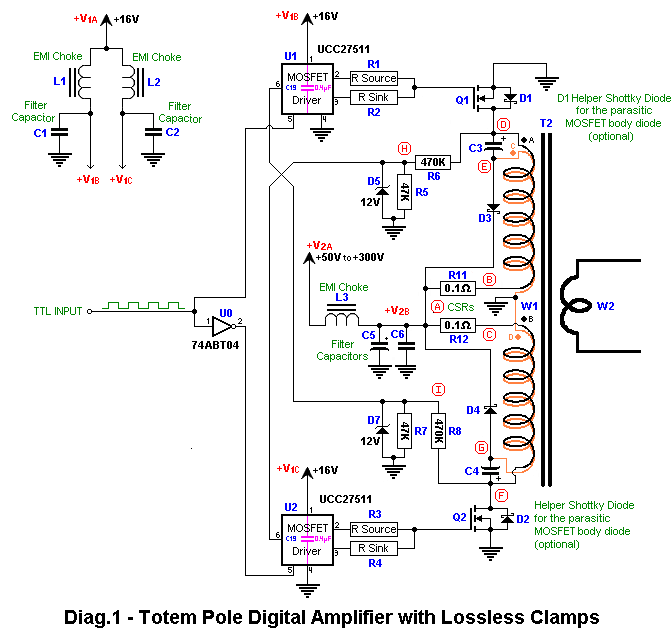
In order not to dissipate the energy of these drain spikes as heat in voltage clamps (a.k.a. snubbers) you can use
lossless clamps instead.
These clamps
recycle the drain spikes' energy
back into the power supply, instead of wasting it in
RC or
Zener or
Transorb "
heaters".

 DESCRIPTION
:
1) Primary windings of T2 are wound bifilarly (e.g. with double-wire speaker cable or two parallel
Litz wires - better).
2) Q1 and Q2 are N-ch power MOSFETs rated for blocking voltages of at least 2*V
2A.
3) Two fast rectifier diodes (e.g. Shottky) are needed for an effective operation of lossless clamps. These diodes (D3 and D4) must be capable of handling the pulsed currents occurring in the primaries (T2,W1
AB) and must be rated for at least 2*V
2A.
4) Two capacitors (C3 & C4) in the μF range (the more μF the better) are used as a floating DC sources (=V
2A) for the lossless clamps. They can be ceramic or electrolytic capacitors (or both types connected in parallel), but must have low-ESR and be rated for at least V
2A.
5) Pins #6 of the UCC27511 drivers (U1 and U2) are used to ensure that two power MOSFETs (Q1 and Q2) are not conducting both at the same time. The voltage on pin #6 must be above 2.4V in order for the driver to be enabled (this happens only when the opposite MOSFET stops conducting. This is sensed by R6 and R8).
6) R11 and R12 are optional Current Sensing Resistors (CSRs) used for troubleshooting (they must be of non-wirewound type and non-inductive!). The waveform across these resistors should have a sawtooth shape. If this waveform is rectangular, then it is an indication of insufficient number of turns in primary windings (too low inductance of T2,W1
ABCD) or an input frequency that is too low. These resistors can also serve as current limiters/fuses that protect Q1 and Q2 from excessive current damage.
7) If the U0
Hex Inverter is used, then all of its unused inputs (pins #3,5,7,9,11,13) must be grounded and its power supply pin #14 must be connected to +5V DC and bypassed with a suitable capacitor to pin #7 (this is not shown on the schematic!). If the U0 inverter is unavailable, instead of it, it might be possible to use an improvised inverter composed of a small BJT (or MOSFET) and additional resistors.
8) Diodes D6 and D9 are used with a low-power isolation transformer (T1) in order to protect the inputs of U1 and U2 from negative voltages (they can tolerate only -0.3V). These diodes can be low current/power but they must have a reverse recovery time (t
rr) that is sufficiently fast to support the maximum input frequency applied to T1.
9) An absence of a varying input signal during the presence of V1
A and W2
A supply voltages will result in
damage to T2,W1
AB windings or Q1,Q2 transistors because T2 is incapable of handling DC applied to its primaries.
10) The rules of connections layout for U1 and U2, described in the
UCC27511 Datasheet in section "PCB Layout" on page 22, should be followed strictly.
P.S.
To maximize the efficiency of lossless clamps, the T2 primary winding W1
A should have the same length, turns and placement as the winding W1
C and should be interleaved with it. By the same token, the winding W1
B should have the same length, turns and placement as the winding W1
D and should be interleaved with it (all of this is automatically ensured when those windings are wound bifilarly with e.g. a speaker cable consisting of two parallel wires). The only permitted difference between the windings is the wire thickness - because windings W1
C and W1
D conduct less average current than W1
A and W1
B, they can be wound with a thinner wire.
Of course, for best results the windings of all toroidal transformers should be wound in 2 layers (or a higher even number) where each layer uniformly covers one full outer circumference of the the core (see
this diagram for what happens if it does not).
Each layer should be advanced in the opposite direction to the next layer (also along the full outer circumference of the core), while keeping the turn direction constant (e.g. CCW) for all layers.
If more layers are needed then use an even number of layers (e.g. 2, 4, 6, 8, etc...) alternating the direction of winding advancement along the circumference of the core, for each successive layer.
On schematics below, the beginning of each wire in the 2-wire bifilar cable, that constitutes the primary windings, is marked with a full dot of a different color.


 feature is available which provides a place all members can chat, either publicly or privately.
 Author
Topic: Comments on the McFreey paper (Read 118038 times)